The core of high-density interconnect boards (HDI), located in vias
The circuit processing of multi-layer PCBs is no different from that of single-layer and double-layer PCBs, but the biggest difference lies in the through hole process.
The circuits are all etched, and the via holes are drilled and then plated with copper. Everyone involved in hardware development understands these, so we won't go into detail.
Multilayer circuit boards typically include through hole boards, first order boards, second order boards, and second order stacked hole boards. Higher level boards such as third-order boards and arbitrary layer interconnection boards are rarely used and are expensive, so we won't discuss them much for now.
The most common through-hole
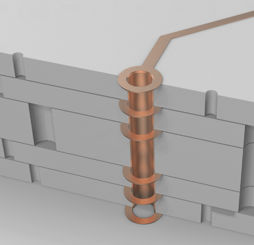
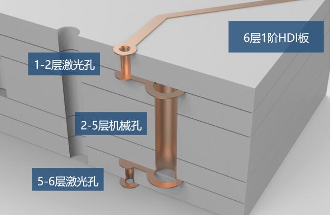
This is a stacked structure diagram of a 6-layer, 1st order HDI board, with laser holes on both surfaces and a 0.1mm inner diameter. The inner layer is a mechanical hole
Equivalent to a 4-layer through-hole plate, covered with 2 layers on the outside.
Laser can only penetrate fiberglass panels, not metal copper. So punching holes on the outer surface will not affect other internal circuits.
After laser drilling, copper plating is carried out to form a laser through hole.
2nd order HDI board with two layers of laser holes
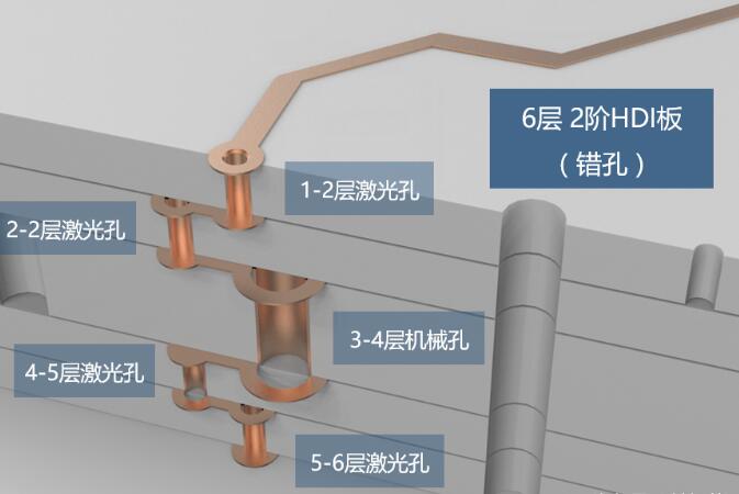
This picture is a 6-layer 2nd order staggered hole HDI board.
The so-called second order refers to having two layers of laser holes
The so-called staggered holes refer to the two layers of laser holes being staggered.
Why should we stagger it? Due to insufficient copper plating, the holes inside are empty, so it is not possible to drill holes directly on top. Instead, a certain distance should be staggered and a layer of empty holes should be added.
6th level 2nd level=4th level 1st level plus 2nd level outside.
8th level 2nd level=6th level 1st level plus 2 levels outside.
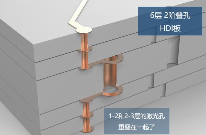
Stacked orifice plates have complex processes and higher prices.
The two layers of laser holes on the staggered hole plate overlap together. The circuit will be more compact.
The inner laser hole needs to be electroplated and filled out, and then the outer laser hole needs to be made. The price is more expensive than the wrong hole.
Super expensive arbitrary layer interconnection board with multi-layer laser hole stacking
Each layer is a laser hole, and each layer can be connected together. Route the wire as you want, and punch the hole as you want.
Layout engineers feel great when they think about it! No longer afraid of not being able to draw!
Purchasing makes me want to cry, it's more than 10 times more expensive than ordinary through hole boards!
So, only products like the iPhone are willing to use them. Other mobile phone brands have never heard of anyone using any layer of interconnection board.
Finally, put in a picture and compare it carefully.
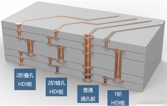
Please pay attention to the size of the hole and whether the pad of the hole is closed or open.
Article source: Headline number/Yi Intelligence. If there is any infringement, please contact us to delete it. Thank you! Contact number 13006659147